Results
Context and overall objectives
Laser-based technologies for creating structures in the range from nanometre up to millimetre size find many applications such as free form optics, photonics, multifunctional surfaces, lab-on-chip, etc. with a global market volume of > 200 billion euros. The original structures, known as masters, are the first step in the making of tools for key-enabling technologies like injection molding or nanoimprinting. Some of the current limitations in the laser lithography processes are the limited depth of the structures, small area and low speed at process level, high-power consumption in the laser interference lithography, and multiple and expensive processes required for the development of hierarchical multifunctional structures at industrial level.
The OPTIMAL project will integrate for the first-time different laser lithography technologies, quality monitoring systems and processes in one platform for the development of structures with high depth, dimensions in the range from 100 nm to sub-mm, 2D&3D shape on flat surface, combining parallel & serial patterning, no need for external treatments on samples, increased speed and large area. The OPTIMAL project uses self-learning algorithms to optimize the virtual photomask as well as integrates methods for an inline control of the laser patterning. The OPTIMAL platform will be validated through the manufacturing of master tools for four different use cases: a) full-polymer micro lenses for industrial optics, b) hierarchical multifunctional drag reduction riblet structures for aviation, c) free-form lens arrays for high-end virtual reality displays and d) microfluidic hierarchical structures for lab on chip medical devices.
Work performed and main achievements
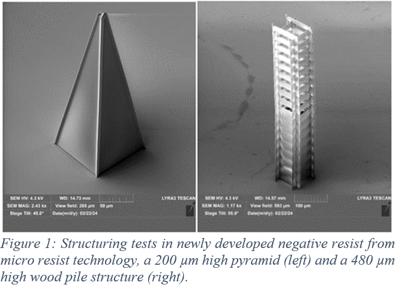
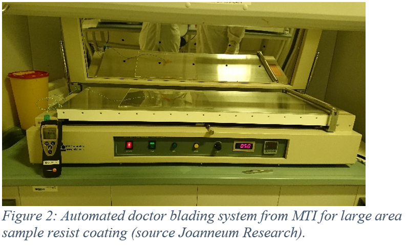
A new positive resist formulation for the generation and grayscale patterning of thick resist layers beyond 100 μm was developed. Its physical parameters, such as viscosity, refractive index and density were determined, and it was lithographically investigated. Thicknesses of up to 120 - 150µm were obtained by single coating, and up to 200 μm by double coating. A negative resist with the highest viscosity currently available allowed the generation of up to 500 μm thick resist layers. Resists with an even higher solids content and viscosity, respectively, as well as with increased resist film transparency are developed. Thicknesses of up to 500 μm were obtained in a single coating technique, and the resists were successfully lithographically patterned by mask aligner and LED exposure. Doctor blading was selected as coating technology to apply the resists on the desired very large area substrates.
The structure specifications for use cases, which will be fabricated to show manufacturing possibilities of the developed OPTIMAL platform, were defined including the features and properties of the structures.
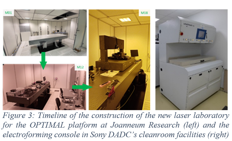
A new laser laboratory to host the OPTIMAL-platform has been gradually prepared. The main components of the OPTIMAL system are an optical table, a customized high-precision XYZ positioning system, a galvo scanner, and two highly efficient lasers with the average output power of 1 W, in particular, a 405 nm cw laser and a 780 nm femtosecond laser. In parallel to this, four writing modules were developed, namely the one photon writing, the two photon writing, the laser interference and the parallel writing module based on a spatial-light modulator. For the replication of the large OPTIMAL masters, a modified electroforming equipment was also developed.
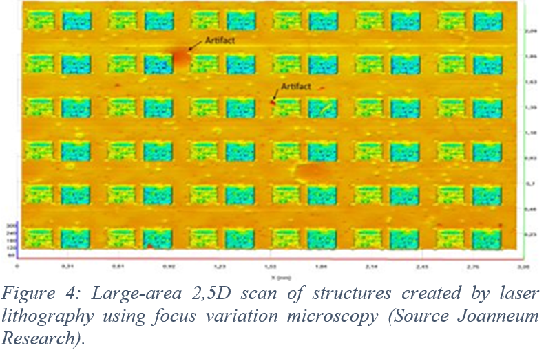
A vision system able to track objects captured by camera is under development and will be integrated into the OPTIMAL platform. System calibration procedures as well as software modules for fast focus determination has been designed and implemented. Several sample illumination concepts were tested for imaging of the surface topography and hardware solutions for parallel and serial writing scenarios has been implemented. New high-resolution camera was developed for focus-variation microscopy, which has been adopted to serial scanning of large samples. Innovative dark-field and diffractive imaging approaches for large-area surface testing were utilized for vision subsystem targeting heterogeneity and sample defects.
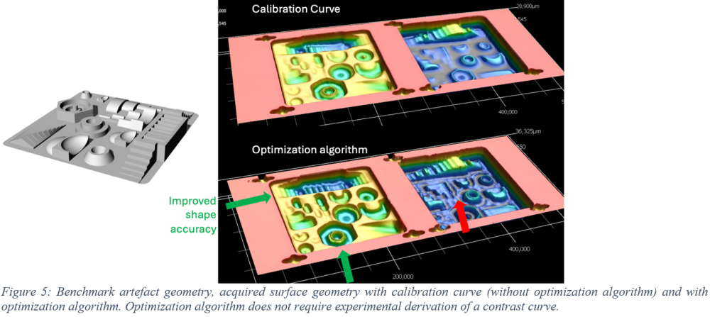
Four benchmark artefacts of varying dimensions and complexity have been developed for efficient acquisition of data required for training self-learning algorithms. Expandable data and metadata libraries comprising all data relating to manufacturing trials have been defined, with the latter made publicly available on the project website for tracking and recording all manufacturing trials. Self-learning algorithms have been developed for optimization of process parameters based on neural network representations of the physical process. The self-learning algorithm has been tested on three occasions, with the final trial leading to an improvement in build accuracy compared to use of a contrast curve.
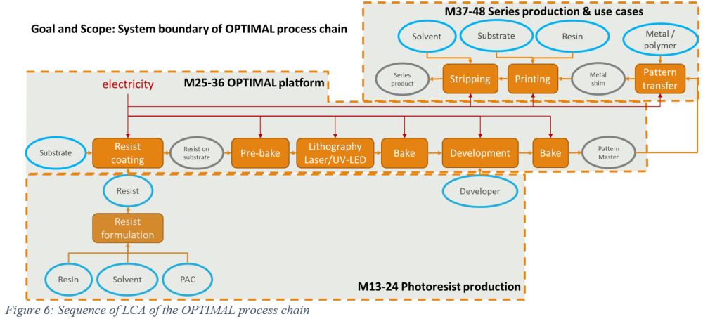
The approach for elaborating the life cycle inventory of resist material manufacturing was developed and applied to first chemical products.
The project’s branding elements, including the logo, presentation, factsheet, brochure, and poster were developed together with the creation and continuous update of the OPTIMAL website (https://www.optimal-project.eu/). The preliminary project results were already presented at several international events. Clustering activities with projects dealing with laser-based innovation and manufacturing are in progress. The preliminary IPR analysis confirm the innovation level of the OPTIMAL results and 14 exploitable results and corresponding exploitation strategies were identified preliminarily. A Data Management Plan was defined together with the day-to-day management procedure for progress monitoring, quality, and risk assessment.
Results beyond the state of the art
New breakthroughs in the field of photoresists are expected with the aim to increase thickness and area while keeping homogeneity. This will open up new market potential.
A reduction of resources (i.e. power consumption) for the LIL module has already been achieved by the accurate selection of the laser source (estimated reduction: 500-1000 times less than current gas laser source). This is in line with the energy saving strategies at modules and components level, already implemented in OPTIMAL. Furthermore, self-learning algorithms will greatly reduce the number of manufacturing trials (“first time right”) that are required for each new build, thus reducing resource consumption, waste, and CO2 emissions.
By accelerating and upscaling the structuring process, the OPTIMAL project will increase the process efficiency and yield, which will allow an increase of productivity, and cost reduction for of the required structures.
The identification of 14 results with exploitation potential, the confirmation of innovation level (results from IPR analysis) and market needs assessed by the members of the OPTIMAL External Advisory Board and contacts established during the industrial oriented events, support the potential economic impact of the project results.
Making the OPTIMAL metadata openly accessible and the collaboration with projects dealing with with laser-based innovation and manufacturing is supporting the skills development for the scientific community and industries and is creating awareness about the use of laser lithography in green manufacturing
The OPTIMAL project has already promoted the creation of new job positions and implementation of safety principles.
 |
 |
 |
 |
 |
 |
Publishable Deliverables and Publications


